
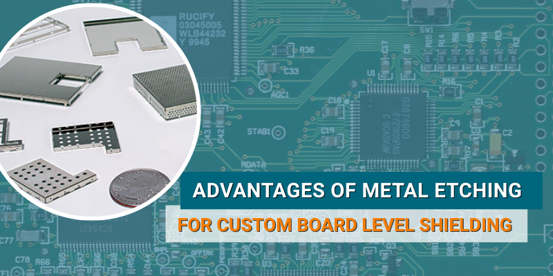
20 Jan The Advantages of Metal Etching for Custom Board Level EMI Shielding Solutions
Board level EMI shielding is imperative in ensuring devices meet performance specifications and regulatory requirements. This is why board level metal-etched EMI shields are often the best fit when you need reliable EMI performance without compromising on size, weight, or manufacturability in compact designs.
One of the most effective methods for producing high-precision, lightweight, and highly custom-fit EMI shields is photochemical etching. Unlike traditional stamping or machining methods, this approach allows for intricate geometries, very thin materials, and rapid iteration without complex tooling. This is optimal for fast-paced electronics development and relatively low volumes.
In this article, I’ll walk you through what metal etching is, the design opportunities it affords, its advantages, and how it compares to other fabrication techniques.
Key Takeaways
- Metal-etched board level shields can closely match PCB layouts, reducing leakage and improving consistency.
- Photochemical etching avoids mechanical stress, helping maintain flatness and accurate edges for better fit and grounding.
- Etching enables complex features in thin metals, like vents, bend lines, and integrated grounding fingers or clips.
- Compared with stamping, laser cutting, and CNC, etching typically needs less tooling, iterates faster, and supports finer details.
Why Board Level Metal-Etched EMI Shields Are a Practical Choice
Board level metal-etched EMI shields are designed to match PCB layouts closely, which helps reduce leakage paths and improves repeatability from prototype to production. Because the process is tooling-light, design updates are easier to accommodate during development and compliance testing. This is especially valuable when you are balancing shielding performance with manufacturability.
What Is Metal Etching in EMI Shielding?
Metal etching, chemical etching, or photochemical etching is a process that uses controlled chemical reactions to remove material from a metal sheet to produce precise patterns. Unlike stamping or CNC machining, which mechanically deform the metal, etching removes material under very precise control, without hard tooling or mechanical cutters and without inducing stress or distortion. For board level EMI shields, this helps maintain flatness and edge accuracy, improving fit and grounding.
Etching is especially well-suited to thin metals such as stainless steel, copper alloys, brass, and nickel silver. Because even slight distortion can affect performance, particularly at soldered edges, etching is a strong option for complex geometries and extremely fine details that are difficult to achieve with traditional fabrication methods.
Design Features Enabled by Metal Etching
The beauty of metal etching lies in the design freedom it allows. In board level metal-etched EMI shields, this design freedom helps you achieve better coverage, easier assembly, and more predictable performance. Some of the features we frequently implement for board level shields include:
- Custom shield geometries and multi-surface shields:Etching allows shields to conform to the contours of your PCB, covering multiple and even stepped surfaces without requiring separate parts.
- Venting and airflow patterns:Helpful in thermal management, perforations and vent patterns can be integrated without compromising shielding effectiveness (feature sizes depending on the emission or sensitivity profile of the shielded areas).
- Fold lines and bend relief features:These make forming easier while preventing stress or cracking in thin metals. \/ and \_/ features enable precise bend formation that is highly predictable.
- Integrated grounding fingers and clips:Ensures reliable electrical connectivity while simplifying assembly. Spring properties vary with base material.
- SMT-compatible designs:Etched shields can be designed for automated pick-and-place assembly, saving time and reducing human error. These are usually presented as “one-piece hand presented” or “bandoliered”, depending on equipment capability and production volumes.
Advantages of Metal Etching for EMI Shielding
When you are specifying board level metal-etched EMI shields, you benefit from several advantages:
Precision, Repeatability and Tight Tolerances
One of the biggest advantages of etching is precision within and between production runs. It can achieve fine features, sharp corners, micro-perforations, and tight tolerances with astonishing reliability and repeatability. For OEMs producing mid-to-high volume boards, this consistency is crucial for maintaining EMI performance across and between batches.
Design Flexibility
Etching allows for adaptive/responsive incorporation of complex shapes, partial cut logos, part numbers, bend lines, venting holes, and integrated multi-level designs – all in a single manufacturing step. Rapid iteration from prototype to production is possible without expensive hard tooling. This flexibility is invaluable when designs change during development or regulatory testing.
Cost Efficiency
Compared to stamping, the tooling costs for metal etching are insignificant – simple optical exposure tools are identical to those used in PCB production. It’s ideal for mid-volume runs or high-mix, low-volume production. If your design changes, you don’t need to invest in new dies; these digital toolings adjust easily, fast, and at low cost.
Material Integrity
Because etching does not mechanically stress or deform the sheet material, the finished shield retains excellent flatness while deriving high rigidity from the forming process. Poorer conductivity stainless steel also does not lose conductivity in the bend zones. Flatness and uniform conductivity are important for sensitive electronics where contact integrity and consistent shielding are high priorities.
Compatibility With Thin Metals
Many modern electronics demand lightweight shielding. Etching works best with very thin stainless steel, copper, nickel silver, and a variety of other alloys, allowing you to save space and weight without compromising EMI protection.
Faster Prototyping and Lead Times
This technically PCB-adjacent process, also intrinsically digital in nature, means quick adjustments and rapid iterations are feasible and carry modest cost consequences. If your development cycles are tight, metal etching helps you get functional prototypes in days rather than weeks.
Comparison: Metal Etching vs Other Fabrication Methods
- Etching vs. stamping:Stamping requires long lead time, high-cost dies, and can deform thin materials in unexpected ways. Etching eliminates all stress and is more cost-effective for low-to-mid volumes, as digital tooling costs are lower. This is one reason photochemical etched board level shielding is often selected for fast-moving electronics programs where revisions are expected.
- Etching vs. laser cutting:Unlike etching, laser cutting introduces heat-affected zones and cannot achieve ultra-fine features in thin metals. Etching also eases manual bending thanks to partially cut V-grooves or perforations, which reduce EMI leakage at joints. Etching provides clean edges and higher precision for intricate designs, while partial etch results in precise and zero-perforation bends.
- Etching vs CNC machining:CNC is excellent for thicker sections or simpler shapes, but it is slow and expensive. For thin sheets or complex micro-features, costs rise very rapidly. Etching handles all of these issues with speed and precision, delivering both low up-front and part costs.
Overall, my experience is that metal etching provides the best balance of precision, flexibility, and cost for board level EMI shields.
Applications in Modern Electronics
These days, board level metal-etched EMI shields are being used in a wide range of applications where performance, space, and weight are critical:
- IoT Devices and wearables:Thin, lightweight shields conform to compact designs without adding wasteful bulk or weight.
- Medical electronics:Reliable shielding is vital for sensitive signals in diagnostic and monitoring equipment.
- Aerospace and defence systems:Etched shields maintain integrity under vibration, thermal cycles, and harsh conditions. They offer high integrity and resilience without adding weight, critical in flight applications.
- Automotive electronics and ADAS:Compact, lightweight shields are essential for modern driver-assistance systems. Performance and cost-efficiency requirements are both met by etched shields.
- Telecom, networking, and 5G components:High-frequency circuits demand high-integrity, precision shielding to prevent signal degradation.
For all of these sectors, well-designed custom etched EMI board shielding ensures your products perform reliably while meeting tight space and regulatory constraints.
Conclusion
Board level EMI shielding is no longer just about dropping a metal cover over a PCB. Today’s devices require precision, lightweight, and highly customized solutions that integrate seamlessly with modern electronics manufacturing. Multi-zone shielding within individual boards increases the challenge.
Whether you’re designing a new IoT device, upgrading automotive electronics, or developing aerospace systems, board level metal-etched EMI shields give you the precision, design freedom, and rapid turnaround you need to stay ahead.
If you need board level EMI shielding that matches tight PCB constraints, we can help you evaluate material options, feature limits, and forming details early, so you get to production with fewer surprises.
You don’t have to compromise on EMI performance. At The ID Group, we specialize in EMI/RFI shielding solutions and can deliver the right technical and cost-performance EMI shields for your application. Contact us for more information.
Now Offering New Enclosure Shielding Gaskets
Board level EMI shielding is imperative in en...
The Advantages of Metal Etching for Custom Board Level EMI Shielding Solutions
Board level EMI shielding is imperative in en...

What is Board-Level EMI Shielding and Why Does It Matter for PCB Design
In the electronics industry, where devices ar...

Custom BeCu Board Level Shielding: Precision Protection for Critical Applications
Electronic systems are steadily becoming fast...

4 Differences Between Thermally and Electrically Conductive Elastomers
Conductive elastomers make a significant cont...

The Role of EMI Shielding in Medical Devices
Conductive elastomers make a significant cont...

Industry-Specific EMI RFI Shielding Applications
As the technology environment becomes increas...

5 Most Common Types of EMI Shielding Gaskets
EMI and RFI interferences are expressions of ...

4 Things to Consider When Choosing a Conductive Elastomer
Conductive elastomers make a significant cont...

The Role of Electrically Conductive Elastomers in EMI Shielding
From properties to composition, explore how e...

7 Benefits of EMI Shielding for Manufacturers
Electromagnetic interference (EMI) is a const...

Why Choose The ID Group for Your EMI RFI Shielding Needs
As owner of The ID Group, I'm proud to say th...

TechEtch 2500 Series: A New Standard in Shielding Effectiveness
In the world of EMI shielding solutions, the ...

Custom Die-Cut Foam Gaskets: Everything You Need to Know
Essential components in various industries, c...

Gasket Materials for Effective Sealing and Protection
Gaskets play a critical role in many of today...

9 Metals and Materials Used in EMI Shielding
Electromagnetic interference (EMI) is a nuisa...

EMI Shielding Fingerstock Gasket Mounting Options—An Overview
Electromagnetic interference (EMI) can affect...

Critical Performance Variables for EMI Honeycomb Vents
As technology evolves, so do the products req...


How Tech Etch Products Help with EMI RFI Shielding Issues
Electronic devices need robust protection fro...

What Is EMI Shielding Effectiveness and How to Measure It?
In order to ensure the proper functioning of ...

What to Know About Beryllium Copper and EMI RFI Shielding
Today, most electronic devices are equipped w...

What is EMI RFI Shielding and How Does it Work?
To understand what is EMI RFI shielding, it i...